4. FPGA pin mapping
The pin mapping of the SoC signals to the board pins is described for each supported board:
4.1. ARTY 100t
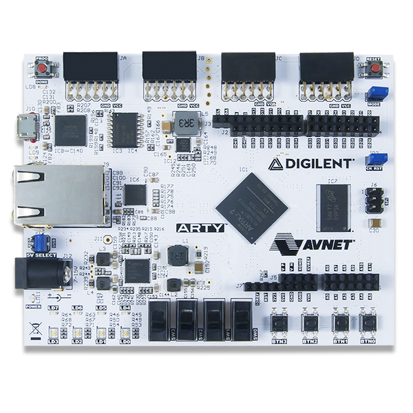
Fig. 4.1 Arty-100t FPGA Board from Digilent
4.1.1. FPGA Board Connector Mapping
The following table shows the pin configuration of ChromiteM SoC on the Xilinx Arty-100T FPGA. The connector group and pin names are as indicated on the Xilinx Arty-100T board.
| Connector Group | Connecter Pin Name | Soc Signal Name |
|---|---|---|
| J3 | IO0 | gpio[0] |
| IO1 | gpio[1] | |
| IO2 | gpio[2] | |
| IO3 | gpio[3] | |
| IO4 | gpio[4] | |
| IO5 | gpio[5] | |
| IO6 | gpio[6] | |
| IO7 | gpio[7] | |
| IO8 | gpio[8] | |
| IO9 | gpio[9] | |
| IO10 | gpio[10] | |
| IO11 | gpio[11] | |
| IO12 | gpio[12] | |
| IO13 | gpio[13] | |
| NA | LD4 | gpio[14] |
| NA | LD5 | gpio[15] |
| NA | SW0 | boot_config[0] |
| NA | SW1 | boot_config[1] |
Note
The serial communication happens using uart0 connected to the FPGA package pins D10 and A9, which communicate to the host system through the micro-USB port (connector J10).
The debug interface of the processor is connected to the Xilinx JTAG tap, which in-turn is time multiplexed with uart0, and is connected to the micro-USB port. This configuration let’s us to not have dedicated JTAG pins, thereby eliminating the need for an external JTAG Debug probe (like J-Link).
Note
The DDR controller (of Xilinx) uses the default pin configuration as specified by Xilinx.