4. Supported FPGAs
The pin mapping of the SoC signals to the board pins is described for each supported board:
4.1. ARTY 100t
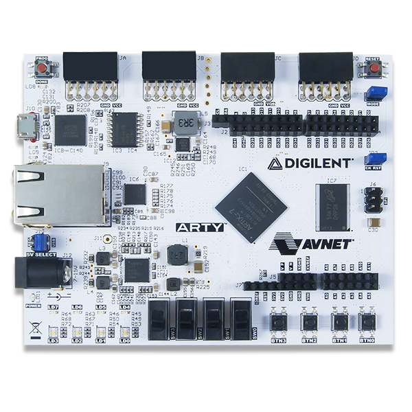
Fig. 4.1 Arty-100t FPGA Board from Digilent
4.1.1. Resource Summary
All values are post implementation:
Closure Frequency : 50MHz
LUT utilization : 84%
BRAM utilization : 57%
LUTRAM utilization : 6%
DSP utilization : 7%
4.1.2. FPGA Board Connector Mapping
The following table shows the pin configuration of ChromiteM SoC on the Xilinx Arty-100T FPGA. The connector group and pin names are as indicated on the Xilinx Arty-100T board.
Connector Group |
Connecter Pin Name |
Soc Signal Name |
|---|---|---|
J3 |
IO0 |
gpio[0] |
IO1 |
gpio[1] |
|
IO2 |
gpio[2] |
|
IO3 |
gpio[3] |
|
IO4 |
gpio[4] |
|
IO5 |
gpio[5] |
|
IO6 |
gpio[6] |
|
IO7 |
gpio[7] |
|
IO8 |
gpio[8] |
|
IO9 |
gpio[9] |
|
IO10 |
gpio[10] |
|
IO11 |
gpio[11] |
|
IO12 |
gpio[12] |
|
IO13 |
gpio[13] |
|
J7 |
A0 |
gpio[14] |
A1 |
gpio[15] |
|
A2 |
gpio[16] |
|
A3 |
gpio[17] |
|
A4 |
gpio[18] |
|
A5 |
gpio[19] |
|
NA |
LD4 |
gpio[20] |
NA |
LD5 |
gpio[21] |
NA |
SW0 |
boot_config[0] |
NA |
SW1 |
boot_config[1] |
NA |
LED0_B |
pwmout[0] |
NA |
LED0_G |
pwmout[1] |
NA |
LED0_R |
pwmout[2] |
J2 |
IO26 |
pwmout[3] |
J2 |
IO27 |
pwmout[4] |
J2 |
IO28 |
pwmout[5] |
J2 |
IO29 |
spi1_mosi |
J2 |
IO30 |
spi1_sclk |
J2 |
IO31 |
spi1_miso |
J2 |
IO32 |
spi1_nss[0] |
J2 |
IO33 |
spi1_nss[1] |
J6 |
5 |
spi2_mosi |
J6 |
2 |
spi2_sclk |
J6 |
3 |
spi2_nss |
J6 |
1 |
spi2_miso |
JA |
1 |
qspi0_mv_ncs_o |
JA |
2 |
qspi0_mv_io_o[0] |
JA |
3 |
qspi0_mv_io_o[1] |
JA |
4 |
qspi0_mv_clk_o |
JA |
9 |
qspi0_mv_io_o[2] |
JA |
10 |
qspi0_mv_io_o[3] |
Note
The serial communication happens using uart0 connected to the FPGA package pins D10 and A9, which communicate to the host system through the micro-USB port (connector J10).
The debug interface of the processor is connected to the Xilinx JTAG tap, which in-turn is time multiplexed with uart0, and is connected to the micro-USB port. This configuration let’s us to not have dedicated JTAG pins, thereby eliminating the need for an external JTAG Debug probe (like J-Link).
Note
The DDR controller (of Xilinx) uses the default pin configuration as specified by Xilinx.
Note
The SPI0 is used to interface flash.
Connector Group |
Value |
Soc Signal Name |
|---|---|---|
SW1:SW0 |
00 |
Debug Mode |
SW1:SW0 |
01 |
Jump to OCM |
SW1:SW0 |
10 |
Jump to DDR |
Note
The ETHLite (of Xilinx) uses the default pin configuration as specified by Xilinx.